 正版
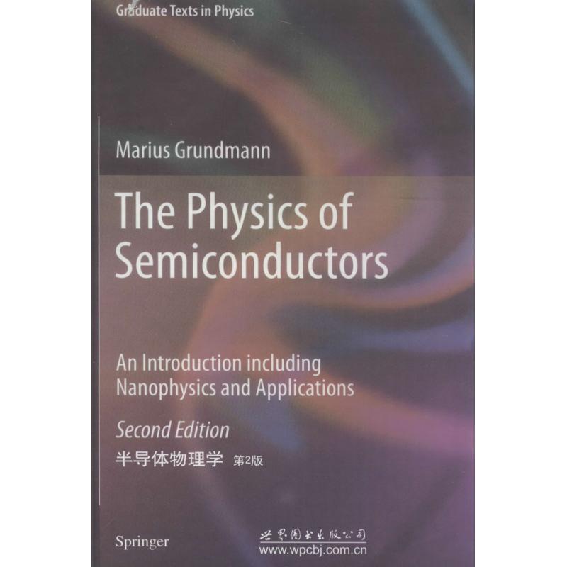
半导体物理学
- 书名
- 半导体物理学
- 作者
- 无 著
- 出版社
- 世界图书出版公司
- 出版时间
- 2014-07-01
- ISBN
- 9787510077814
- 货号
- 1201005299
- 品相
- 全新
- 分类
- 当代·哲学思想
- 书名
- 半导体物理学
- 作者
- 无 著
- 出版社
- 世界图书出版公司
- 出版时间
- 2014-07-01
- ISBN
- 9787510077814
- 货号
- 1201005299
- 品相
- 全新
- 分类
- 当代·哲学思想
目录▼
1 Introduction
1.1 Timetable
1.2 Nobel Prize Winners
1.3 General Information
Part 1 Fundamentals
2 Bonds
2.1 Introduction
2.2 Covalent Bonds
2.2.1 Electron—Pair Bond
2.2.2 sp3 Bonds
2.2.3 sp2 Bonds
2.3 Ionic Bonds
2.4 Mixed Bonds
2.5 Metallic Bonding
2.6 van—der—Waals Bonds
2.7 Hamilton Operator of the Solid
3 Crystals
3.1 Introduction
3.2 Crystal Structure
3.3 Lattice
3.3.1 Unit Cell
3.3.2 Point Group
3.3.3 Space Group
3.3.42D Bravais Lattices
3,3.53D Bravais Lattices
3.3.6 Polycrystalline Semiconductors
3.3.7 Amorphous Semiconductors
3.4 Important Crystal Structures
3.4.1 Rocksalt Structure
3.4.2 CsCl Structure
3.4.3 Diamond Structure
3.4.4 Zincblende Structure
3.4.5 Wurtzite Structure
3.4.6 Chalcopyrite Structure
3.4.7 Fluorite Structure
3.4.8 Delafossite Structure
3.4.9 Perovskite Structure
3.4.10 NiAs Structure
3.4.11 Further Structures
3.5 Polytypism
3.6 Reciprocal Lattice
3.6.1 Reciprocal Lattice Vectors
3.6.2 Miller Indices
3.6.3 Brillouin Zone
3.7 Alloys
3.7.1 Random Alloys
3.7.2 Phase Diagram
3.7.3 Virtual Crystal Approximation
3.7.4 Lattice Parameter
3.7.5 Ordering
4 Defects
4.1 Introduction
4.2 Point Defects
4.2.1 Point Defect Types
4.2.2 Thermodynamics
4.2.3 Diffusion
4.2.4 Dopant Distribution
4.2.5 Large Concentration Effects
4.3 Dislocations
4.3.1 Dislocation Types
4.3.2 Visualization of Dislocations by Etching
4.3.3 Impurity Hardening
4.4 Extended Defects
4.4.1 Micro—cracks
4.4.2 Stacking Faults
4.4.3 Grain Boundaries
4.4.4 Antiphase and Inversion Domains
4.5 Disorder
5 Mechanical Properties
5.1 Introduction
5.2 Lattice Vibrations
5.2.1 Monoatomic Linear Chain
5.2.2 Diatomic Linear Chain
5.2.3 Lattice Vibrations of a Three—Dimensional Crystal
5.2.4 Density of States
5.2.5 Phonons
5.2.6 Localized Vibrational Modes
5.2.7 Phonons in Alloys
5.2.8 Electric Field Created by Optical Phonons
5.3 Elasticity
5.3.1 Thermal Expansion
5.3.2 Stress—Strain Relation
5.3.3 Biaxial Strain
5.3.4 Three—Dimensional Strain
5.3.5 Substrate Bending
5.3.6 Scrolling
5.3.7 Critical Thickness
5.4 Cleaving
6 Band Structure
6.1 Introduction
6.2 Electrons in a Periodic Potential
6.2.1 Blochs Theorem
6.2.2 Free—Electron Dispersion
6.2.3 Kronig—Penney Model
6.2.4 Lattice Vector Expansion
6.2.5 Kramers degeneracy
6.3 Band Structure of Selected Semiconductors
6.3.1 Silicon
6.3.2 Germaruum
6.3.3 GaAs
6.3.4 GaP
6.3.5 GaN
6.3.6 Lead Salts
6.3.7 Chalcopyrites
6.3.8 Delafossites
6.3.9 Perovskites
6.4 Alloy Semiconductors
6.5 Amorphous Semiconductors
6.6 Systematics of Semiconductor Band Gaps
6.7 Temperature Dependence of the Band Gap
6.8 Electron Dispersion
6.8.1 Equation of Electron Motion
6.8.2 Effective Mass of Electrons
6.8.3 Polaron Mass
6.8.4 Nonparabolicity of Electron Mass
6.9 Holes
6.9.1 Hole Concept
6.9.2 Hole Dispersion Relation
6.9.3 Valence—Band Fine Structure
6.1 Strain Effect on the Band Structure
6.10.1 Strain Effect on Band Edges
6.10.2 Strain Effect on Effective Masses
6.10.3 Interaction with a Localized Level
6.11 Density of States
10.2.3 Stimulated Emission
10.2.4 Net Recombination Rate
10.2.5 Recombination Dynarrucs
10.2.6 Lasing .
10.3 Exciton Recombination
10.3.1 Free Excitons
10.3.2 Bound Excitons
10.3.3 Alloy Broadening
10.4 Phonon R,eplica
10.5 Self—absorption
10.6 Donor—Acceptor Pair Transitions
10.7 Inner—Impurity Recombination
10.8 Auger Recombination
10.9 Band—Impurity Recombination
10.9.1 Shockley—Read—Hall Kinetics
10.9.2 Multilevel Traps.
10.1 Field Effect
10.10.1 Thermally Activated Emission
10.10.2 Direct Tunneling
10.10.3 Assisted Tunneling
10.11 Recombination at Extended Defects
10.11.1 Surfaces
10.11.2 Grain Boundaries
10.11.3 Dislocations
10.12 Excess—Carrier Profiles
10.12.1 Generation at Surface
10.12.2 Generation in the Bulk
……
Part 2 Selected Topics
Part 3 Applications
文摘▼
本书是一部分讲述半导体物理学的教材,为高年级本科生、研究生学习这门学科提供了大量丰富的材料,使得读者能够进入更深层次的学习和研究。一方面,这部教材是固态物理学和半导体物理之间的一个很好的平衡;另外一方面,是各种各样的半导体设备和它们在电子和光子设备中应用的很好展示。书中强调了半导体,如合金、异质结构、纳米结构等领域的实际应用方面,这些都是半导体物理学研究不可或缺,但又常常被忽略。书中也包罗了一些更高层次的话题,如Bragg错误、共振腔、极化和磁性半导体。本教材中给出许多结果的公式推导,这样可以更好理解这门科目。学习半导体物力学需要极少的固态物理学知识即可。这是第二版,较第一版许多内容得到了扩展,并且在深度上也有所增加,如掺杂剂扩散、纳米线、有机半导体的重组、多连接极细胞、量子点、和有机LED、薄膜晶体管、基于碳的纳米结构和透明导电氧化物。